The Fastest delivery ability of high precision PCB manufacturer !
Language:
FAQs
Certificates
The advantages of flexible printed circuit board

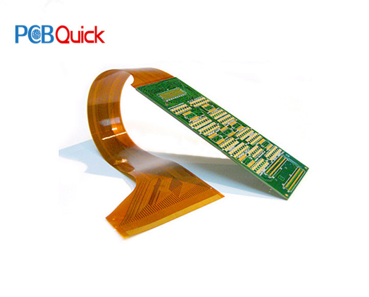
Flexible printed circuit boards and rigid flexible circuit boards are extremely durable, reliable, and allow you to design circuits that fit the device rather than build the device that fits the circuit board. That is why the design is created upon receipt of specifications That meet the purpose of the final product.
Why flexible PCB
Encapsulation: unlike a normal PCB, a flexible PCB can be placed almost anywhere, saving space and reducing the weight of a wired solution. In fact, a flexible PCB can save up to 60 percent of the weight and space of a rigid printed circuit board. Flexible printed circuit boards are thin and light and can be folded and positioned to miniaturize electronic devices. Skilled flexible circuit board technicians can use tweezers and fine tip soldering irons to manually weld very small parts under a microscope.
Durability and reliability: flexible printed circuit boards reduce the number of interconnections required, which means less soldering and contact bonding. This will leave fewer potential sources of failure, thus improving the reliability of the equipment. In addition the ductility and low quality of the flexible circuit board can significantly reduce the impact of vibration and improve the performance. Polyimide is known for its excellent thermal stability, which enables the equipment to withstand extremely high heat. As a result, flexible circuits are commonly used in military and medical applications. The main cause of circuit board failure may be related to environmental pressure. However, these can be easily avoided when using and storing devices under appropriate conditions. Unlike most rigid circuit boards, flexible circuits can be made of materials more suitable for harsh environments.
Cost saving: using flexible printed circuit board, the overall finished product assembly package size and material cost is low. Flexible circuits also reduce wiring errors and test times, thus reducing additional costs.
Flexible PCBS can be found in many common household items. Your mobile phone, computer, TV, clock and microwave oven all use FPC. Medical technologies such as scanners and X-ray machines, cars, GPS navigation devices and military technology also use flexible PCBS because they have many advantages over other circuit boards.
Flex Design Basics
–Static: Not meant to flex.
–Flex to Install: Only meant to flex on limited basis. To install or replace and repair.
–Dynamic: Depending on flex construction and conditions this could result in >1M flex cycles.
Terminology
•Back Bared Pads / Back Side Access - This is a flex that is typically single sided in construction but has the copper accessed from both sides.
•Conductor aspect ratio - Relationship of conductor width to conductor height. General rule of thumb is conductor width should be greater then 5 times the conductor thickness.
•Coverfilm / Coverlay -This is the insulating material, usually in a film format, that is laminated to the flex circuit to define solderable areas. Can be drilled, laser cut or chemically removed to create complex geometries.
•Dynamic –A type of flexible circuit that will see repeated flexing, sometimes more than 1 million cycles, such as in a disk drive, mobile phone or laptop computer.
•Hold Down Tabs -These are extensions of the copper pad and are used to help anchor the pad during soldering processes both in assembly and rework.
•I-Beam Effect -This is the result of stacking your conductors during your design.Subsequent flexing induces stress and compression, causing cracking to occur.
•PIC, Photoimagable Coverfilm / Coverlay -This is another means of defining your solderable areas. This material is apply in a clean room environment, exposed with an artwork and then developed. This allows for complex geometries not available from routing or other soft tooling means.
•PSA (Pressure Sensitive Adhesive) -An adhesive used to bond stiffeners to specific regions of the flex circuit.

I-Beam Effect
Always try to avoid “stacking traces” in the same location from layer to layer.
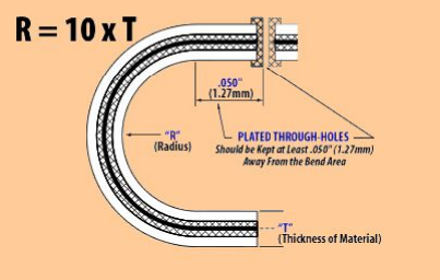
Calculating Minimum Bend Radius
The general guideline for calculating minimum bend radius is 10X the total thickness of the flexible circuit for double sided (2 layer) applications.
The general guideline for calculating minimum bend radius is 6X the total thickness of the flexible circuit for single sided (1 layer) applications.
The general guideline for calculating minimum bend radius is 20X -25X the total thickness of the flexible circuit for multi-layer (3+ layers) applications.

CONTACT US
- Name:
- Mary
- Tel:
86-0755-29518736
- Email:
- mary@kfquickpcb.com
- WhatsApp:
- https://wa.me/8613632989860
- Skype:
- Skype:pcbquick
- Address:
- Building D, Xintai Industrial Park, Xitou Second Industrial Zone, SongGang Town,Bao'an,Shenzhen,China
FOLLOW US
Please send your message to us
- *Title
- *Content
MOBILE WEB
Focus on mobile phone clients
QR code

subscription
