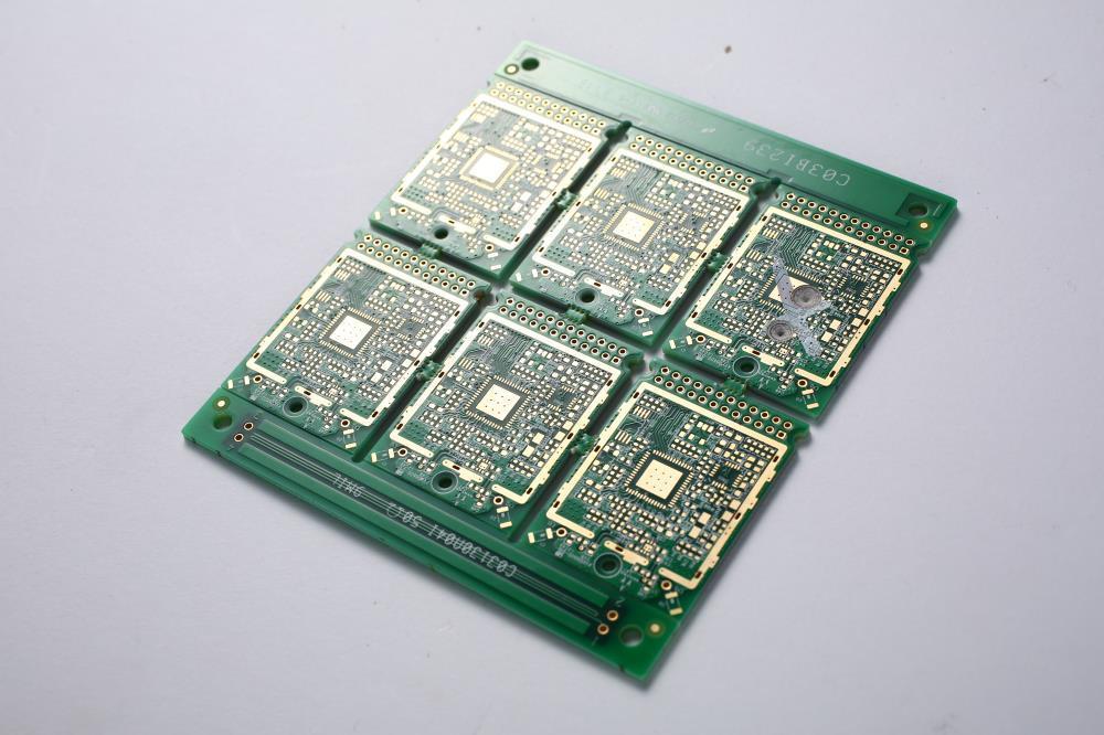
Multilayer PCB Design
Traditional PCB consists of non-conductive substrate materials – frequently glass fiber epoxy construction – paired with a layer of conductive elements such as copper on one or two sides (single or double-sided boards). Electronic components are placed on the boards and soldered in place, making a connection through means of drilled thru holes or STM assembly. Either one or two sides board may be utilized for the mounting of components.
Due to the physical attributes of these PCBs, large boards may be largely used in customized circuit size or application, or even the use of multiple boards.With the advent and development of technology and manufacturing techniques, which is a great leap in electronics applications.
Multilayer pcb design with many strategic advantages:
1.Space requirements – adding layers means the board thickness will be increased (depending on the numbers of layers) Considering that adding layers generates only a slight increase in thickness of the resulting board (depending on the number of layers), which may require bigger space to loading multilayer pcb. This is critical for modern electronic devices
2.Weight – just like space benefits, combining layers of components into a single multi-layer card can provide circuit functionality with a fraction of the weight over prior technologies.There are Some disadvantages of Multilayer PCB Design
3.Replacements – due to the structure and complexity of multilayer pcb design, factory may manufacture some failed and imperfect boards. In most cases, when workers meet these kinds of printed circuit board, they usually replace a failed pcb board, rather than attempt repair.
Technology Supports of PCB Copy & PCB Design
PCB design software is very helpful for computer-aided design (CAD) that increase efficiency, find error and problem areas quickly, and generate files for fabricators. Furthermore, the design files can be analyzed for missing or incorrect content, avoiding traditional manufacturing questions and issue back-and-forth communications.
Design for Manufacturing (DFM) applications help both designers and fabricators to validate manufacture-ability of the resulting design by analyzing functions. Without a DFM tool, PCB designs will be impractical, costly, or even impossible to build as designed.
Computer Aided Manufacturing (CAM) software is used by the manufacturer to validate and automate the actual fabrication processes.
All in all, these sophisticated tools make multilayer PCB design and manufacturing more efficient, streamlining the multilayer pcb manufacture process.

Maybe it’s helpful to you:
Web link
Previous
Something about V-CUT

