Conventional Lamination Structure and Impedance Design of Four Layer PCB Board
With the increasingly complex circuit design,How to ensure the integrity of various signals (especially high-speed signals)That is to ensure signal quality,Become a problem.At this point, the need to use the transmission line theory analysis, the control signal line characteristic impedance matching as the key, not strict impedance control, will lead to considerable signal reflection and signal distortion, resulting in design failure.Common signals, such as PCI bus, PCI-E bus, USB, Ethernet, DDR memory, LVDS signals, etc., require impedance control. Impedance control eventually need to achieve through the PCB design, PCB board technology also put forward higher requirements.
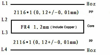
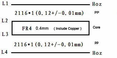
The following will introduce our conventional four-layer board thickness of the laminated structure and some common impedance calculation results, customers in need can be based on the following recommended parameters design impedance line width, spacing:
The above four kinds of laminating structure is our company 4layer laminates conventional laminated structure,can be seen from the figure, conventional laminated structure with PP are 2116, a thickness of about 0.12mm.
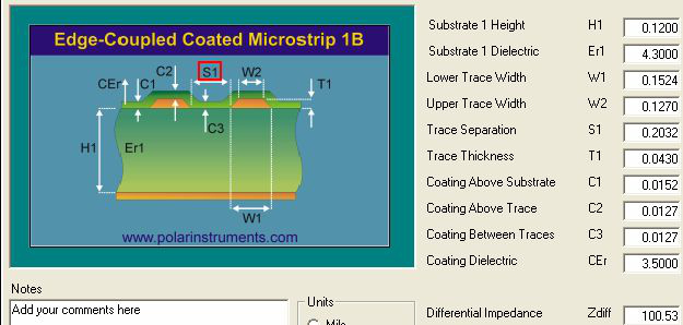
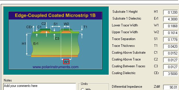
According to the conventional laminated structure of our company, the following parameters can be referred to the parameters of the conventional impedance lines (for example, the L2 impedance line of the L1 layer and the L3 reference impedance line of the L4 layer)
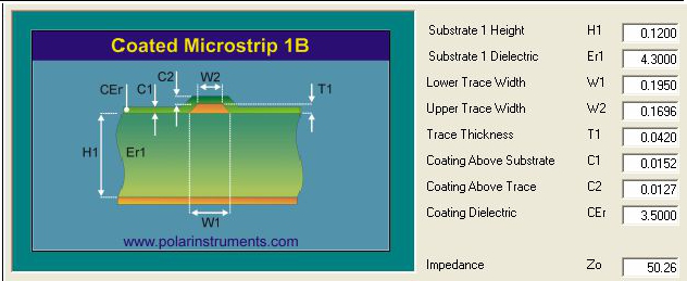
Outer line width 0.195mm, control single-ended impedance 50 +/- 10% ohms (L1 Ref L2, L4 Ref L3)
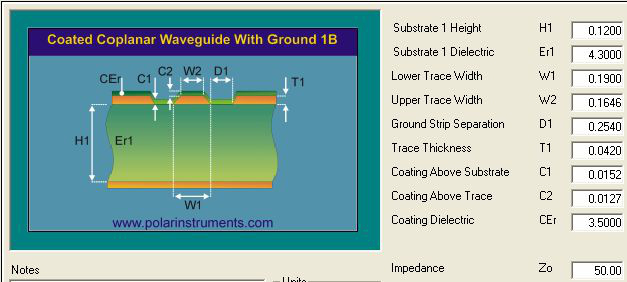
Double-sided wire width 0.19mm, wire-to-copper pitch 0.254mm, controlling single-sided coplanar impedance 50 +/- 10% ohms (L1 Ref L2, L4 Ref L3)
