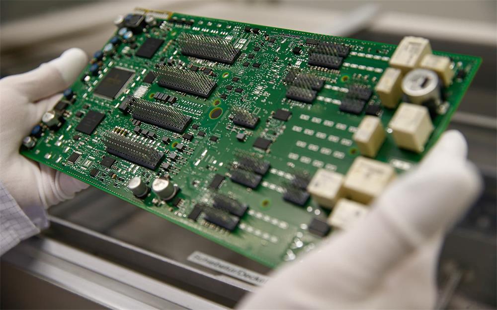
The Process of Printed Circuit Board Wiring

For users who are new to printed circuit board design, the first problem they face is the steps involved in the design work. Therefore, you must understand the basic process before designing a printed circuit board, that is, the following wiring process of the printed circuit board.
1. Drawing the correct schematic diagram and network table schematic diagram is the prerequisite for designing the PCB board, and the network table is the bridge connecting the schematic diagram and the PCB board diagram, so you must first get the correct schematic diagram and network before drawing the surface of PCB circuit board.
2. Determine the component packaging to complete the conversion from the schematic to the PCB. Only knowing the connection relationship of each component object is not enough. You must also know the packaging of each component. Before importing the netlist file, you must load the PCB component package library first, and make sure that all used libraries have been loaded.
3. Users who set environmental parameters can set environmental parameters according to their own habits, such as grid size, cursor capture size, conversion of metric and imperial units, and the color of the working level. In addition, because the PCB board drawing consists of many layers, it is also necessary to set the layers of the PCB board.
4. This step for planning the circuit board is mainly to set various physical parameters of the circuit board, including whether the circuit board adopts a double-layer board or a multi-layer board, the shape and size of the circuit board, and the installation method of the circuit board. Put an appropriate size pad on the hole, and draw the outline of the PCB board on the forbidden wiring layer, etc.
5. The netlist contains the packaging form of each component and the connection relationship between the components, so after importing the netlist, the basis for the subsequent design of the PCB is obtained.
6. The layout of components should be comprehensively considered in terms of mechanical structure, heat dissipation, electromagnetic interference, and the convenience of future wiring. First, layout the components related to the mechanical size and lock these components, then lay out the larger and more space-consuming components and the core components of the circuit, and finally layout the peripheral small components.
7. Formulate detailed wiring rules. Wiring rules include wiring spacing, various line widths, via size, wiring topology, etc. These rules need to be set according to the actual situation of the designed circuit board. In addition, place filling layers in areas where wiring is not desired, such as the wiring layer underneath the radiator and the lying two-pin crystal oscillator.
8. PCB wiring includes three small steps: manual wiring, automatic wiring, and manual adjustment.
9. The processing of the lead-out end of the circuit board In the actual PCB design, the power supply, grounding, signal input, and output must be connected to the outside world, and the lead-out method depends on the process requirements. Common lead-out method-use the pad to lead out and use the connector to lead out. It is also possible to add lead-outs in the schematic diagram and then update the PCB board.
10. Copper coating is to enhances the anti-interference ability of the circuit board. The ground wire network of each wiring layer needs to be copper-coated. According to the needs, there can be grid-shaped copper or solid copper, or the power network can be copper-coated.
11. In order to ensure that the circuit board diagram complies with the design rule and all the networks have been correctly connected, the design rule check must be done after the wiring is completed. This step corresponds to the previous formulation of detailed wiring rules. On the one hand, wiring errors can be checked according to the formulated design rules. On the other hand, if some errors need to be ignored during the wiring process, the design rules can also be modified.
12. After adjusting all the information on the remaining layers and passing the design rule check, drag and drop all the characters of the silkscreen layer to the appropriate position. Be careful not to place them under the components or on the vias and pads. For those that are too large, The characters can be reduced appropriately.
13. Save and export the printed board files. After the circuit board design is completed, the printed board files must be sorted, archived, and printed drawings. In addition, you can export the component list, generate a spreadsheet file as a component list, and so on.
The wiring of the PCB needs to be determined according to the composition of the components and the actual application scenarios. If you want to learn more about printed circuit boards after reading the above content, you can get a comprehensive solution by contacting us.
As a professional PCB product manufacturer, we have accumulated rich design and production experience in this field. We have a standardized production department and a strict quality inspection system, which can control the quality of our products in an all-round way. At the same time, we will provide thoughtful one-stop service and effective solution technology according to the actual needs of customers. If you want to buy our printed circuit boards, please contact us immediately!

