Is It Necessary to Plate Copper on the Pcb?

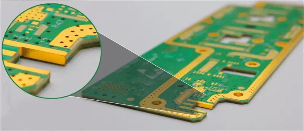
When the printed circuit board is finally grounded, it is usually realized by plating copper. Plating copper can increase the grounding area, make the grounding firm, and signal return smoothly. However, the copper paving treatment does not bring absolute benefits, and we still need to decide according to the design of the PCB. The followings are the pros and cons of copper paving and the types of circuit boards that are applicable.
The advantages of copper coating on the outer layer of the PCB are as follows:
(1) Provide additional shielding protection and noise suppression for the inner signal.
(2) Improve the heat dissipation capacity of the PCB.
(3) In the PCB production process, the amount of corrosive agent is saved.
(4) Avoid the PCB warping and deformation caused by the different stress generated when the PCB is over-reflowed due to the unbalanced copper foil.
Doing so will also bring some disadvantages:
(1) The outer copper-clad plane must be separated by the surface components and signal lines. If there is a poorly grounded copper foil (especially the thin and long copper), it will become an EMI problem.
(2) If the component pins are fully connected with copper, the heat will be lost too quickly, and it will be difficult to desolder and rework.
(3) As mentioned earlier, the copper-clad surface of the outer layer must be well-grounded, and more vias need to be punched to connect to the main ground plane. If more vias are punched, it will inevitably affect the wiring channels, unless blind vias are buried.
For two-layer printed circuit boards, a copper coating is necessary. Generally, the ground plane is laid on the bottom layer, and the main components and power lines, and signal lines are placed on the top layer. For high-impedance circuits, analog circuits (analog-to-digital conversion circuits, switch-mode power conversion circuits), copper plating is a good practice.
For high-speed digital circuits on multi-layer boards with complete power and ground planes, note that this refers to high-speed digital circuits, and copper-cladding on the outer layer will not bring great benefits.
For digital circuits using multi-layer boards, the inner layer has a complete power supply and ground plane, and copper coating on the surface layer does not significantly reduce crosstalk. On the contrary, the copper skin that is too close will change the impedance of the microstrip transmission line. Discontinuous copper skin will also cause the negative impact of discontinuous impedance on the transmission line.
For multi-layer boards, the distance between the microstrip line and the reference plane is less than 10 mils, and the return path of the signal will directly choose the reference plane under the signal line instead of the surrounding copper because its impedance is lower. For a double-layer board with a 60 mil distance between the signal line and the reference plane, a complete copper skin along the entire signal line path can significantly reduce noise.
Therefore, whether or not to pave copper on the surface layer should depend on the application scenario. In addition to sensitive signals that need to be grounded, if there are many high-speed signal lines and components, a lot of small and long copper fragments are generated, and the wiring channels are tight, it is necessary to avoid perforating the surface copper skin to connect with the ground plane. At this time, the surface layer You can choose not to lay copper.
If there are few surface components and high-speed signals, the board is relatively open. For PCB processing requirements, you can choose to lay copper on the surface, but pay attention to the distance between the copper skin and the high-speed signal line to avoid changing the characteristic impedance of the signal line.
PCB QUICK designs and produces a variety of printed circuit boards with excellent craftsmanship, and provides users with thoughtful assembly and solutions. If you want to know more about the circuit board after reading the above, you can get comprehensive and professional information by contacting us.
As a professional PCB product manufacturer, we have accumulated rich manufacturing experience in this field. We have a professional production team and strict quality inspection system, and we have formulated comprehensive and detailed solutions for the production and assembly of products. We can also continuously optimize and adjust the plan according to customer needs, and provide customers with thoughtful one-stop service. If you are interested in our printed circuit boards, please contact us immediately!

