The Fastest delivery ability of high precision PCB manufacturer !
FR4 double layer printed circuit board PCB with Factory Price
FR4 double layer printed circuit board PCB with Factory Price
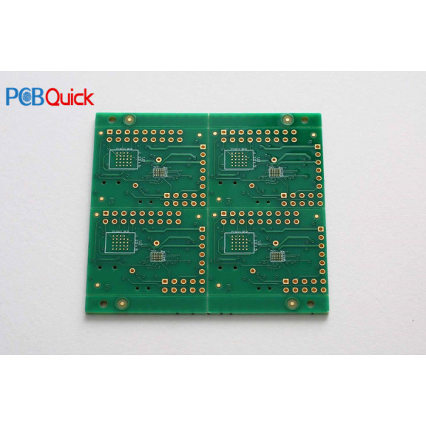
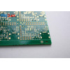
FR4 double layer printed circuit board PCB with Factory Price
Product Description
Material: FR4
Board Thickness: 1.6mm
Copper Thickness: 50um
Soldermask Color: Green
Silkscreen Color: White
Surface Technics: ENIG
Min Holes:0.2mm
Min Line Width and space:5mil/5mil
FR4 Made Ability
| NO | Item | Craft Ability |
|---|---|---|
| 1 | Surface Finishh | HASL,Immersion Gold,Gold Plating,OSP,Immersion Tin,etc |
| 2 | Layer | 2-30 layers |
| 3 | Min. Line Width | 3 mil |
| 4 | Min. Line Space | 3 mil |
| 5 | Min. Space between Pad to Pad | 3 mil |
| 6 | Min.Hole Diameter | 0.10 mm |
| 7 | Min. Bonding Pad Diameter | 10 mil |
| 8 | Max. Proportion of Drilling Hole and Board Thickness | 1:12:5 |
| 9 | Max. Size of Finish Board | 23 inch*35 inch |
| 10 | Rang of Finish Board's Thickness | 0.21-7.0 mm |
| 11 | Min. Thickness of Soldermask | 10 um |
| 12 | Soldermask | Green,Yellow,Black,White,Red,Transparent photosensitive solder mask,Strippable solder mask |
| 13 | Min. Linewidth of Idents | 4 mil |
| 14 | Min. Height of Idents | 25 mil |
| 15 | Color of Silk-screen | White,Yellow,Black |
| 16 | Date File Format | Gerber file and Drilling file,Report series,PADS 2000 series,Powerpcb series,ODB++ |
| 17 | E-testing | 100% E-Testing:High Voltage Testing |
| 18 | Material for PCB | High TG Material:High Frequence (ROGERS,TEFLON,TADONIC,ARLON):Halogen-free Material |
| 19 | Other Test | Impedance Testing,Resistance Testing,Microsection etc |
| 20 | Special Technological Requirement | Blind&Buried Vias and High Thickness Copper |
PCB Quality Requirement
1.on-time delivery:≥97%
2.double layer board acceptability≥99%
3.four-layer board acceptability:≥98%
4.six-layer board acceptability:≥97%
5.eight-layer board acceptability:≥97%
6.ten-layer board acceptability:≥95%
7.customer satisfaction :≥90%
8.complaint rate/rejected rate:≤ 3%
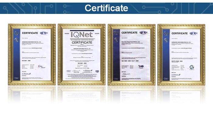
PCB Certificates
UL, TS16949, ISO14001, ISO9001-2008, and RoHS
2L PCB FAQ
Q: What the package of the products?
A: We use vacuum packaging.
Q: Do you accept PCB design with different boards on the same panel?
A: Of course, we can do different boards on the same panel.
Q: What kind of surface treatment process do you adopt on my double layer PCB boards?
A: Such as ENIG, Plating Gold, HAL-LF, Chem.Tin, Chem.Ag and OSP.But on you double-sided pcb usually uses immersion gold.
Q:How long does it take to deliver my design double-sided pcb printed circuit board?
A:Actually,double layer pcb sample fastset delivery time is 24 hours,and mass production is 5 days.
Q:What color is the solder mask of double layer pcb board?
A:The solder mask of double sided pcb is green.
Q:What color is the silkscreen of 2L pcb board?
A:The silkscreen of double-sided pcb is green.
- *Title
- *Content
- Name:
- Mary
- Tel:
86-0755-29518736
- Email:
- mary@kfquickpcb.com
- WhatsApp:
- https://wa.me/8613632989860
- Skype:
- Skype:pcbquick
- Address:
- Building D, Xintai Industrial Park, Xitou Second Industrial Zone, SongGang Town,Bao'an,Shenzhen,China
- *Title
- *Content
Focus on mobile phone clients


