The Fastest delivery ability of high precision PCB manufacturer !
Language:
Home / All / Rigid PCB Manufacturing / Double Sided PCB Manufacturing /
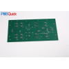
Double Layer PCB Board for LED pcb board design
Double Layer PCB Board for LED pcb board design


Detail Information
Double Layer PCB Board for LED pcb board design
Product Description
Material: FR4
Board Thickness: 1.6mm
Copper Thickness: 50um
Soldermask Color: Green
Silkscreen Color: White
Surface Technics: ENIG
Min Holes:0.2mm
Min Line Width and space:5mil/5mil
FR4 Made Ability
| NO | Item | Craft Ability |
|---|---|---|
| 1 | Surface Finishh | HASL,Immersion Gold,Gold Plating,OSP,Immersion Tin,etc |
| 2 | Layer | 2-30 layers |
| 3 | Min. Line Width | 3 mil |
| 4 | Min. Line Space | 3 mil |
| 5 | Min. Space between Pad to Pad | 3 mil |
| 6 | Min.Hole Diameter | 0.10 mm |
| 7 | Min. Bonding Pad Diameter | 10 mil |
| 8 | Max. Proportion of Drilling Hole and Board Thickness | 1:12:5 |
| 9 | Max. Size of Finish Board | 23 inch*35 inch |
| 10 | Rang of Finish Board's Thickness | 0.21-7.0 mm |
| 11 | Min. Thickness of Soldermask | 10 um |
| 12 | Soldermask | Green,Yellow,Black,White,Red,Transparent photosensitive solder mask,Strippable solder mask |
| 13 | Min. Linewidth of Idents | 4 mil |
| 14 | Min. Height of Idents | 25 mil |
| 15 | Color of Silk-screen | White,Yellow,Black |
| 16 | Date File Format | Gerber file and Drilling file,Report series,PADS 2000 series,Powerpcb series,ODB++ |
| 17 | E-testing | 100% E-Testing:High Voltage Testing |
| 18 | Material for PCB | High TG Material:High Frequence (ROGERS,TEFLON,TADONIC,ARLON):Halogen-free Material |
| 19 | Other Test | Impedance Testing,Resistance Testing,Microsection etc |
| 20 | Special Technological Requirement | Blind&Buried Vias and High Thickness Copper |
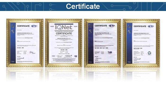
PCB Certificates
UL, TS16949, ISO14001, ISO9001-2008, and RoHS

Related Products
Please send your message to us
- *Title
- *Content
CONTACT US
- Name:
- Mary
- Tel:
86-0755-29518736
- Email:
- mary@kfquickpcb.com
- WhatsApp:
- https://wa.me/8613632989860
- Skype:
- Skype:pcbquick
- Address:
- Building D, Xintai Industrial Park, Xitou Second Industrial Zone, SongGang Town,Bao'an,Shenzhen,China
FOLLOW US
Please send your message to us
- *Title
- *Content
MOBILE WEB
Focus on mobile phone clients
QR code

subscription


